
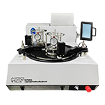

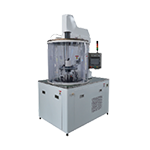


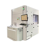


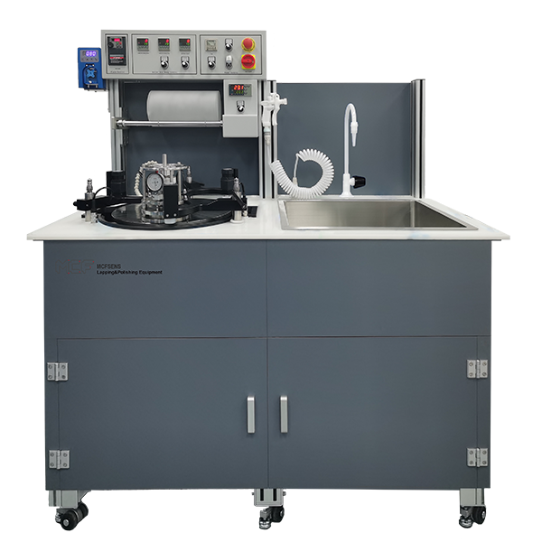
In today's rapid development of the optical communication industry, the lapping and polishing machine, as the core equipment of precision manufacturing, provides key process support for the processing of III.-V semiconductor materials such as gallium arsenide and indium phosphide and lithium niobate modulators.
In view of the strict requirements of optical chips for sub-micron surface roughness and nanometer flatness, the high-precision lapping and polishing machine realizes the accurate correction of wafer thickness errors through multi-level pressure control and flatness control system.
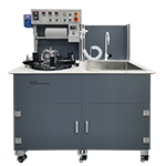
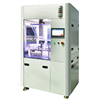
In the manufacture of lithium niobate modulators, its original chemical mechanical polishing(CMP)The process can simultaneously complete the wafer thinning and surface passivation, so that the roughness of the electrode contact surface can be stably controlled0.2nm hereinafter to significantly improve the efficiency of electro-optical modulation. The large-scale application of this equipment in the fields of 5G optical modules and high-speed coherent optical devices has successfully increased the lapping and polishing yield of optical chips to 99.6%, injecting strong momentum into the high-performance manufacturing of optical communication devices.


 Please Leave Us a Message on the Right