
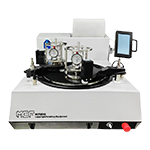


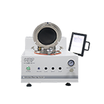
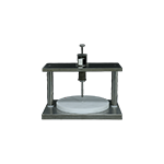


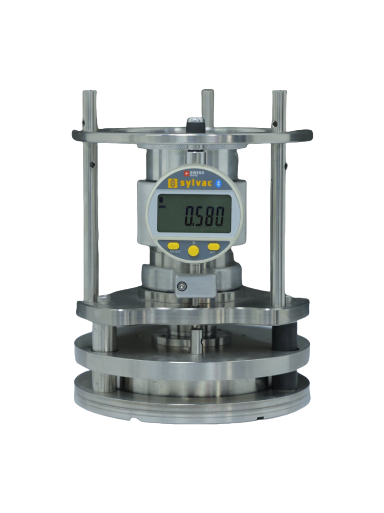
Flatness measurement system FMS200
-
Maximum detectable sample diameter: 200 mm

-
Suitable for measuring non-reflective surfaces in the semiconductor industry
-
Each fringe corresponds to a height of 0.8 μm
-
Supports measurement of surfaces with roughness up to 500 nm
-
Rapid
-
non-destructive measurement


 Please Leave Us a Message on the Right