


GaAs wafer lapping and polishing solutions
客户样品初始状态:
材料:砷化镓;尺寸:4寸;形状:圆形;厚度:600um;粗糙度:500nm;TTV:8um
加工后指标要求:
厚度:80±5um;粗糙度:≤3nm;TTV:≤4um;无划痕及损伤
工艺解析:
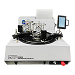
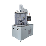
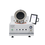
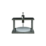
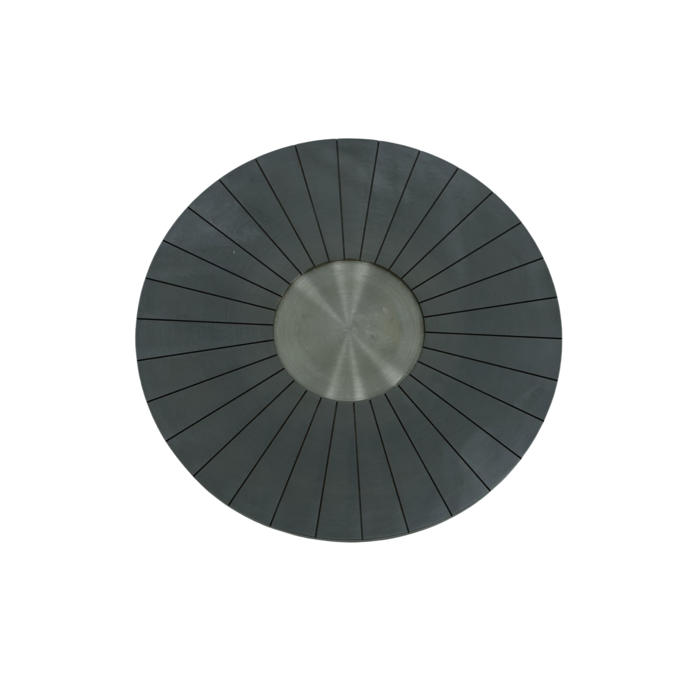
Step1 lapping Stage:Using our GNAD-T series equipment, equipped with grooved glass lapping discs, lapping pressure 60–80 g/cm², rotation speed 20–50 rpm, and alumina powder (particle size 3–10 μm) as the lapping slurry, the wafer thickness can be quickly removed to achieve the goal of rapid thickness removal
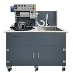
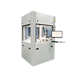
STEP2 rough throwing stage:With our GNAD-T series equipment, equipped with stainless steel polishing discs combined with soft polishing pads (such as polyurethane or flannel), a special alumina mixture with smaller particle sizes, reduces the pressure to 30-60 g/cm² and rotates at 30–60 rpm, reducing the surface roughness to Ra 2–5 nm
Step3 Final polishing treatment: Based on Step2, replace the silica sol polishing slurry and further polish to a roughness of <1nm
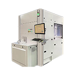
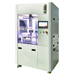
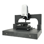
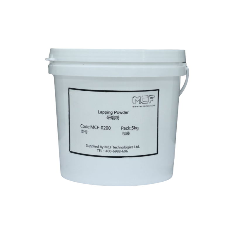
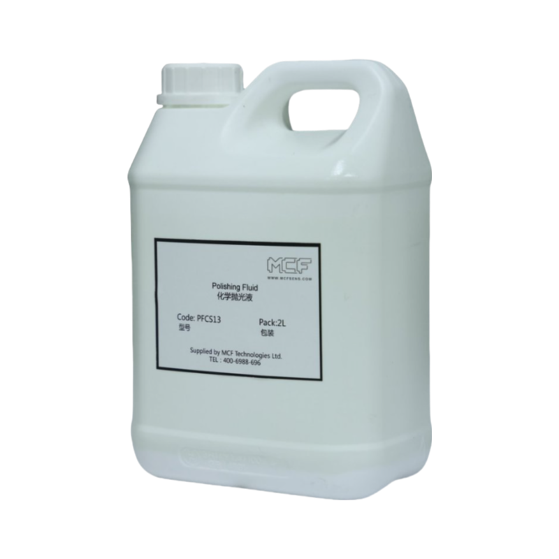
Case supporting host and consumables:GNAD-T lapping and polishing machine, AMS series gluing machine, alumina lapping powder, chemical polishing slurry, silica sol polishing slurry and polyurethane polishing pad, etc
Customer feedbackThe selection of our supporting machines and consumables can achieve the required indicators in batches and stably and gradually optimize the process improvement indicators.


 Please Leave Us a Message on the Right