


本文内容摘取于苏州焜原光电有限公司,发明专利申请文件。
(54)发明名称
半导体材料的抛光方法、用于锑化镓衬底抛光的抛光液
(57)摘要
本发明是针对采用现有技术CMP工艺对锑化镓等较软的半导体材料抛光时抛光磨料、抛光液中含有的金属离子等易附着在被抛光物的表面,使抛光物表面产生划痕、抛光液的寿命低的不足,提供一种半导体材料的抛光方法、用于锑化镓衬底抛光的抛光液,方法是对莫氏硬度为1 .5‑6的半导体材料进行抛光 ,第一步为粗抛光,采用含有硬磨料的抛光液对半导体材料衬底片进行机械抛光,第二步为中抛光,中抛光液包括软抛光磨料、弱酸性氧化剂、有机酸、亲水性非离子表面活性剂、去离子水;第三步为精抛光,精抛光液包括弱酸性氧化剂、有机酸和去离子水,采用本发明的抛光方法对半导体材料进行抛光,消除蚀坑、划痕,减少凹坑,得到表面粗糙度良好的材料。
[0066] Example 1
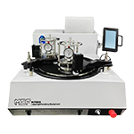
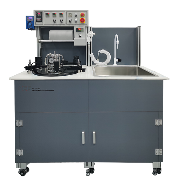
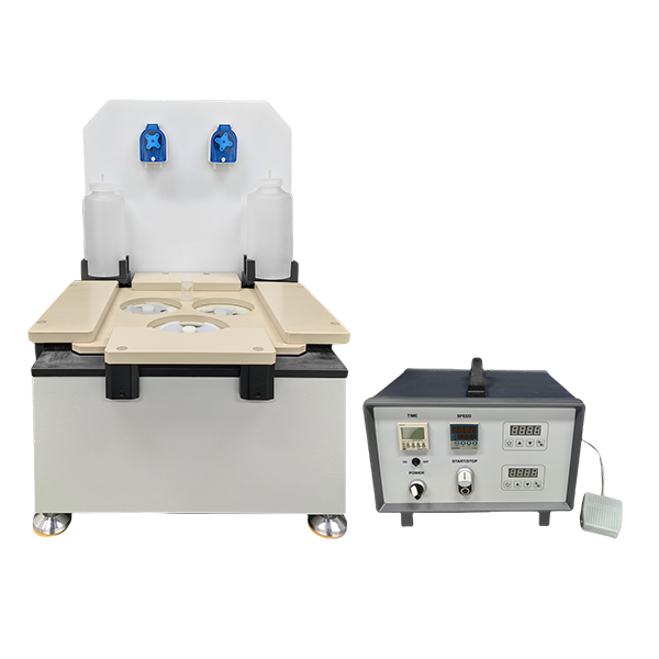
[0067]Using Gnad41 lapping and polishing machine for polishing.
[0068] The process of gallium antimonide substrate includes lapping, chamfering, polishing, and cleaning, the present invention mainly describes the polishing process.
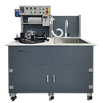
[0069] Removing gallium antimonide wire cutting sheet surface line marks first, lapping to the required thickness of the process, lapping generally single-sided removal thickness of 40-50um; Then the ground gallium antimonide wafer is cleaned with cleaning agent and ultrasonic to ensure that the surface is free of particles generated during gallium antimonide lapping; Heat the φ50.8±0.5mm gallium antimonide wafer evenly on the quartz carrier plate with solid paraffin heating at 60-80 °C, cool and compact, ensure that the TTV is ≤2-3um, ensure that the total thickness deviation accuracy of the subsequent polishing is within a controllable range, wipe off the excess paraffin on the quartz carrier plate, around the wafer and on the surface of the wafer with a dust-free cloth dipped in isopropyl alcohol (IPA) or anhydrous ethanol to prevent the paraffin from contaminating the polishing pad during polishing, and then rinse it with deionized water. Then the polishing process begins.
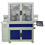
[0070] 第一步粗抛光:粗抛光采用聚氨酯抛光垫,抛光液中含有粒径为3um的氧化铝磨料,压力60g/cm2,转速40rpm,采用roller pump非循环滴液(真空挤压)的方式供给抛光液,说明书 7/19 页10CN 112701037 A10流量80ml/min。粗抛光使用的抛光液按体积百分比由以下组分组成:3um粒径氧化铝磨料10%;亲水性非离子表面活性剂脂肪醇聚氧乙烯醚0 .5%;去离子水89 .5%;
[0071]The second step of polishing: using polyurethane polishing pad, polishing slurry containing a particle size of 60nm silica nanoabrasives and hypochlorous acid, pressure 100g/cm2, speed 80rpm, using roller pump non-circulating dropping (vacuum extrusion) way to supply polishing slurry, flow rate 5ml/min; The polishing slurry used in medium polishing is composed of the following components by volume percentage: 60nm particle size silica 20%; Organic acids were citric acid 0.1%; The oxidant uses hypochlorous acid 7%; hydrophilic nonionic surfactant fatty alcohol ethoxylate0.5%; deionized water 72.4%; The pH value of the polishing slurry ratio is 4 .5.
[0072] 第三步精抛光:精抛光采用带绒毛合成革抛光布,抛光液为无磨料抛光液,压力50g/cm2,转速50rpm,采用roller pump非循环滴液(真空挤压)的方式供给抛光液,流量10ml/min。精抛光使用的抛光液按体积百分比由以下组分组成:氧化剂采用次氯酸1 .5%;有机酸采用柠檬酸0 .5%;去离子水98%;抛光液配比PH值4 .5;
[0073] 化学机械抛光之后,迅速使用去离子水对石英盘上的锑化镓晶片进行喷淋,一是防止氧化,二是进一步去除颗粒污染物,然后进行合适的去蜡、清洗、甩干工序。
[0074] 将本实施例抛光完成后的锑化镓晶片进行如下检测:
[0075] 将抛光完成后的锑化镓晶片在强光下进行目检检测,表面无划伤,无抛光雾,无崩边缺陷;
[0076] 将抛光完成后的锑化镓晶片进行金相显微镜的检测,在暗场100倍下观察晶片表面无亮点、划伤,在明场100、200、500倍下观察晶片表面无凹坑、无蚀坑,无橘皮和划伤,且表面基体非常平整;见附图1。注意,本图像中视野里面的亮点是颗粒污染物并非凹坑,因清洗时未洗干净或测试时环境因素带来的颗粒污染物。
[0077] 将抛光完成后的锑化镓晶片进行surfscan6200颗粒度检测仪的检测,在G6检测范围内52个颗粒/cm2;优于通常的100‑200个颗粒/cm2。见附图3。
[0078] 将抛光完成后的锑化镓晶片的粗糙度Ra进行AFM检测,扫描范围是10um﹡10um,检测值为Ra=0 .19nm,RMS=0 .472nm;见附图5。
半导体材料的抛光方法、用于锑化镓衬底抛光的抛光液


 Please Leave Us a Message on the Right