


The top priority is core technology and industry applicability.
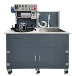
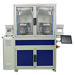
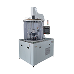
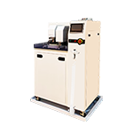
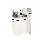
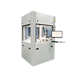
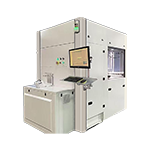
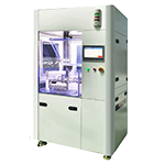
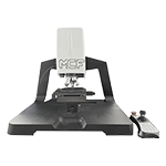
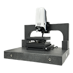
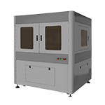
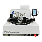
Wafer lapping and polishing requires extremely high equipment precision. It’s essential to assess the manufacturer’s technological depth in the semiconductor industry. Beijing MCF Semiconductor Technology Co., Ltd. specializes in ultra-precision surface processing for semiconductor substrates and wafer manufacturing. Its full-line 8-inch SiC substrate lapping and polishing equipment and fully automated CMP machines can accommodate processing of various substrate materials such as SiC and silicon, with a clear technology focus.
When selecting, check if the manufacturer offers targeted solutions based on wafer size (e.g., 4", 6", 8") and material properties (e.g., hardness, brittleness), to ensure the equipment aligns with your production needs.


 Please Leave Us a Message on the Right