


On April 8-11, 2024, an annual compound semiconductor industry event——2024 Jiufengshan Forum & China International Compound Semiconductor Industry Expo (JFSC&CSE)will be held at Wuhan Optics Valley Science and Technology Convention and Exhibition Center.
Beijing MCF Semiconductor Technology Co., Ltd will appear at this event, and sincerely invite industry colleagues to visit Booth A204 , exchange and cooperation.
Welcome!
JFSC&CSE 2024
尊敬的业界同仁:您好!
Beijing MCF Semiconductor Technology Co., Ltd sincerely invite you to attend the "2024 Jiufengshan Forum and China International Compound Semiconductor Industry Expo" will be held at Hubei Wuhan Optics Valley Science and Technology Convention and Exhibition Center on April 9-11.We look forward to friends from all walks of life to visit and negotiate at Booth A204. On April 9th, Wuhan Optics Valley, see you or disperse!
About Beijing MCF Semiconductor Technology Co., Ltd
Since its establishment, Beijing MCF Technical Ltd. has always been committed to the R&D and manufacturing of precision lapping and polishing equipment and related testing equipment, as well as in-depth research on material treatment processes.
In 1998, MCF established a process technology center in Glasgow, Scotland, to develop lapping and polishing and related processes for high-precision semiconductor materials.
In 2009, MCF set up a precision lapping and polishing machine production line in the university town of Glasgow to develop machines for lapping and polishing and related applications such as III.-V., optoelectronics, infrared materials, etc.
In 2021, MCF Co., Ltd. copied the British production line to set up the first machine assembly line in China, and greatly increased the localization rate of the machine.
With the continuous development and growth of the company, it is in the leading position in the world in terms of material treatment and process surface treatment technology, and has become a modern equipment manufacturing and well-equipped process development company. The company not only provides reliable hardware, but also provides process solutions, after years of development and accumulation, MCF has become a pioneer in advanced semiconductor material processing process and equipment manufacturing.
部分产品介绍
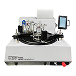
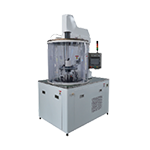
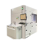
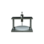
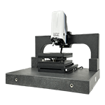
1.MP series four-station lapping and polishing machine
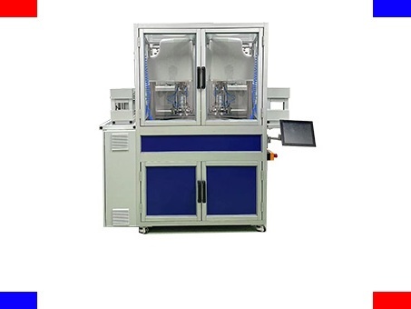
The MP series lapping and polishing machine is an ideal lapping and polishing system for high-volume lapping and polishing processes on wafers of various materials (SiC, GaN, AlN, Sapphire...), components, etc., such as filter materials, wedge materials, liquid crystal display sheets.
Four-motor driven, four oversized polishing heads allow up to 48 2" wafers to be polished simultaneously. Therefore, the MP series is ideal for use in a full-load production environment.
The automatic control panel of the MP series is controlled by a portable touch screen, and the process parameters can be freely entered and changed.
The automatically controlled and intelligent loading/unloading system allows for fast polishing of wafers to reach epitaxial ready surfaces. This system is particularly useful for working with hard substrate materials, and it is also capable of working with wafers up to 8"ø.
MP系列机台优点:
•减少抛光时间 每个抛光头50Kg负载,抛光时间可减少70%。
•多功能和多样性 可抛光多种材料,足够给高精度抛光提供更高的效率和产能,并且可以根据用户的确切要求制作不同的抛光模板,取得最佳成效。
•高产量 一次最多可抛光48片2英寸晶片。
•操作和维护方便、简单 自动化面板控制,全部参数设置都在面板上操作,简单、明了。另装有智能的装载/卸载系统,容易操作。
•易于移动 整个系统安放在可以锁定的轮上,方便固定和移动。
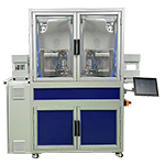
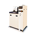
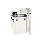
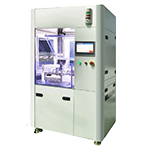
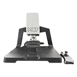
2.WBS430系列自动粘片机
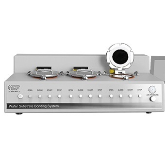
MCF全自动粘片机可以处理薄的和易碎的II-VI 及 III-V族半导体晶片,如硅,碳化硅,氮化镓,砷化镓,磷化铟,碲锌镉,碲镉汞等。实验室粘结这些材料需要保持样品产量的高质量,减少这些昂贵材料在制备过程中的破损。
•全自动工艺循环,减少操作输入;
•极好的晶片与支撑板之间的平行度;
•工艺菜单;
•无气泡粘结;
•样品容量4”, 6”,8”,12”
•单片或多片
MCF全自动粘片机就是为了满足这种高质量贴片要求而设计的。粘片机设计有单头或三头,并配有真空和压力粘结装置。可以让操作者一次粘结三片或一整片直径4”, 6”,8”,12”晶片。
此系列机台能生产对支撑板平行度高标准的晶片,可粘结非标准形状,不同尺寸,不同厚度的晶片。通过集成触控面板,能精确的对所有工艺参数进行控制。这包括一个程序化的粘结温度和真空,以产生对特殊样品种类所需要的环境。
通过精确控制粘片机工艺腔内柔软的隔膜,可以很好的减少极薄或易碎晶片的碎裂,实现粘结厚度的重复性和粘结出尺寸精度极好的样品。隔膜能确保晶片以某种控制方法被压入到蜡中,以提供一个一致且平行的缓冲垫来保护晶片和它的器件。这种设计能确保样品和器件结构不直接与支撑板接触。
粘结过程:晶片室抽空,加热,加压粘结,冷却,整个过程可以由机台全自动运转在45分钟内完成。根据不同材质样片对粘片工艺温度的不同要求,工艺时间会适时调整。
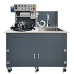
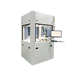
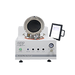
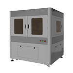
3.CMP设备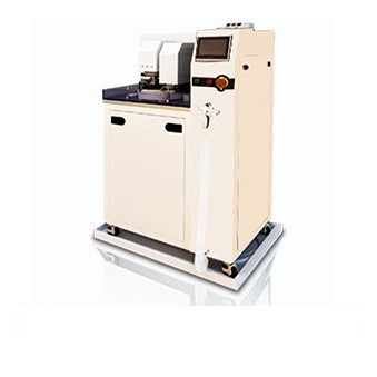
ACDP Auto系统是多用途化学抛光机,它专门设计用于对几何精确度和表面质量要求严格的CMP和除层抛光应用,可获得致亚纳米级水平的Ra。
该设备既可对单个模具进行纳米级的精确抛光,也可对直径大至8英寸的薄片进行抛光,此外,它还可用于那些非传统的抛光应用领域,如硬质基底抛光,Epi表面制备和晶片回收改进。
可供选择的独立水柜,可用于输送及存储抛光液和去离子水或其它液体。这些液体可用于样片移开处理区之前的晶片及模具的喷淋清洗。这个水柜可以和CDP主机连接在一起,给室内没有容器和输送系统的用户提供方便的选择。
为了使ACDP系统尽可能适用多种尺寸样品工艺用途,MCF生产了一系列不同规格型号的夹具,适用于接受最大直径为 8inch 的晶圆或组件。其中,ACDP400配置较小的4 inch直径夹具作为标准配备,而ACDP800配备标准的8”直径夹具。
为了使CDP系列机台适应多种材质不同工艺要求,MCF技术人员根据用户技术要求定制设计相应的抛光模板,以精确地满足ACMP工艺要求。
为了确保在ACDP机台上抛光的晶圆或器件可以得到精确测量和控制,MCF开发了EPD系统,其定制设计的ACDP扫描图形程序可以在笔记本电脑上运行。该程序监控和图形绘制抛光过程,一旦达到终点就自动停止。
防止过度抛光。ACDP扫描还可以作为一个安全功能。如果检测到任何一个被监控的工艺参数发生变化,ACDP Sca将触发音频警报,以帮助防止过度抛光。这方面的例子比如载波速度从其预设值被改变。EPD系统会注意到这种情况的发生,因为衬垫和被抛光材料之间的摩擦水平会因载体速度的任何改变而改变,这将足以危及晶圆/ IC的成功平坦化,此时,EPD系统将在从衬垫表面移除夹具之前触发声音警报,也可设置成自动停机。


 Please Leave Us a Message on the Right